Alnilam
A desktop PCB fabricator: the board you design by day is in your hands the next morning
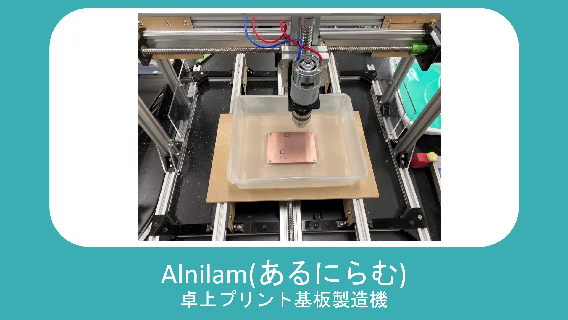
- Science Castle 2021: 5th THK Award, Best Development Award and Encouragement Award
- Geekten 2022: Grand Prize, Hardware and Embedded Category
- Selected for the NEDO NEP Kaitaku Course (2026)
Overview
A machine that fabricates double-sided printed circuit boards on a desktop within a few hours. Think of it as a 3D printer for circuit boards. I started the project after suffering through week-long waits for outsourced boards at high school robotics competitions. After winning the THK Award at Science Castle and the grand prize at Geekten, the project was selected for the NEDO NEP Kaitaku Course, and I am now pushing it toward commercialization.
Background
When I was developing Bellatrix, my RoboCupJunior robot, printed circuit boards had to be outsourced to overseas factories. Shipping was expensive, and each order took a week to arrive. Development stopped in the meantime. The pace of trial and error is the engine of development, yet the boards alone kept stalling it, every single time. And this was not just my problem: students entering robotics competitions and researchers iterating on prototypes are forced into the same wait.
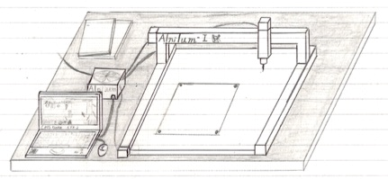 A sketch of the finished machine, drawn at the concept stage
3D printers transformed enclosure design by letting you print and test a shape the same day you think of it. If board fabrication could likewise be completed on a desktop, the trial-and-error cycle would spin faster and development by students and researchers would accelerate dramatically. No machine on the market could do it, though. If it did not exist, I would build it myself. That decision was the start of Alnilam.
The machine
 A through-hole: a vertical hole connecting the traces on the front of a board to those on the back
The hardest part of fabricating double-sided boards is establishing conduction through the through-holes that connect the front traces to the back. Existing desktop CNC machines cannot handle this step, and the industrial equipment that can costs millions of yen and requires dedicated facilities for handling chemicals. Alnilam solved this with a combination of machining and chemical processing.
The process has three stages. First, a GRBL-based CNC mills the copper foil to form the traces, and the same machine also handles drilling and edge cuts. Next, electroless copper plating with a proprietary chemical solution establishes conduction through the holes. No ready-made procedure existed for this chemical step, so I brought a chemist I knew onto the team, and we established it from scratch through literature research and repeated experiments. Finally, electrolytic refining and a resist treatment complete the board.
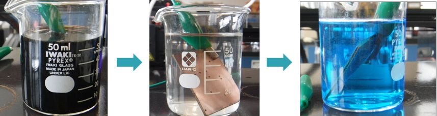 The electroless plating step that establishes conduction through the holes
 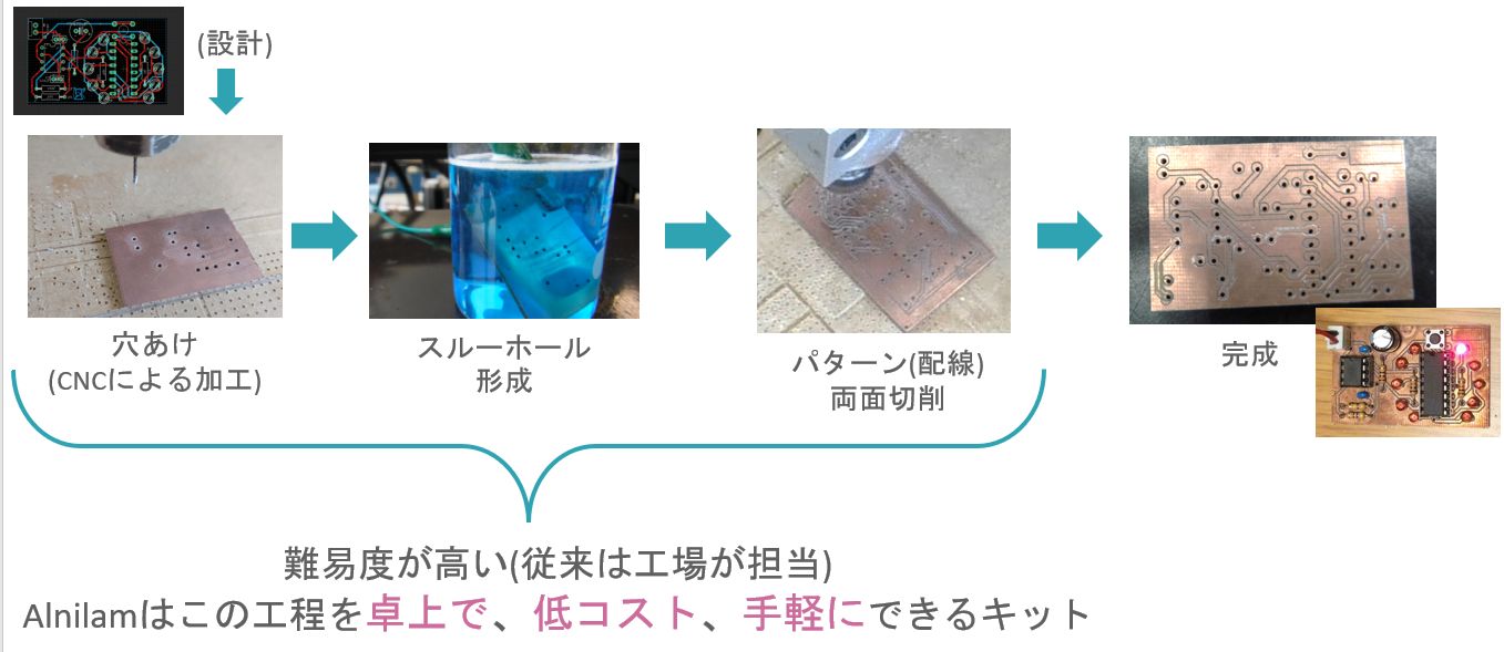 Process flow for fabricating a double-sided printed circuit board
 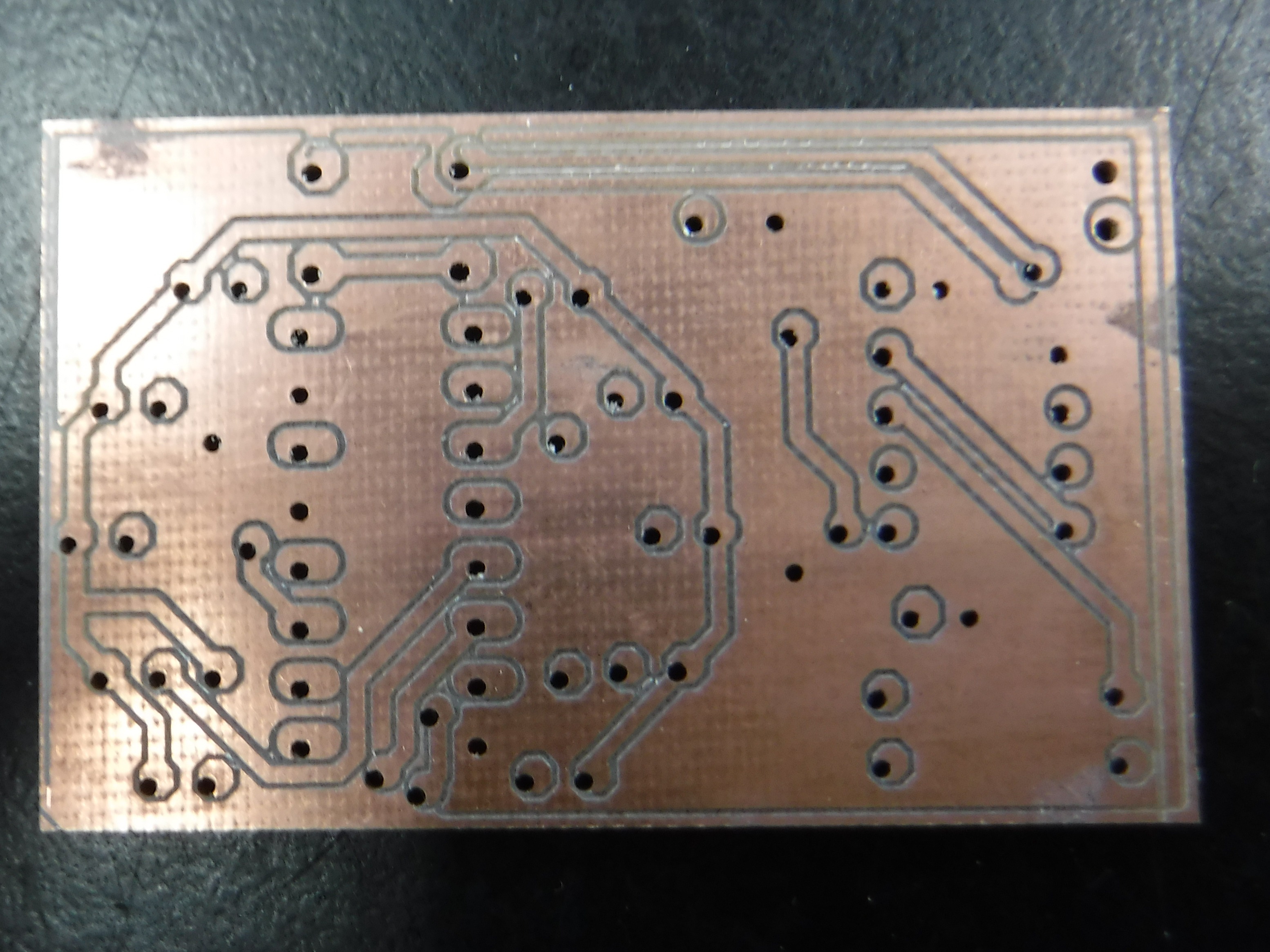 A printed circuit board machined with Alnilam
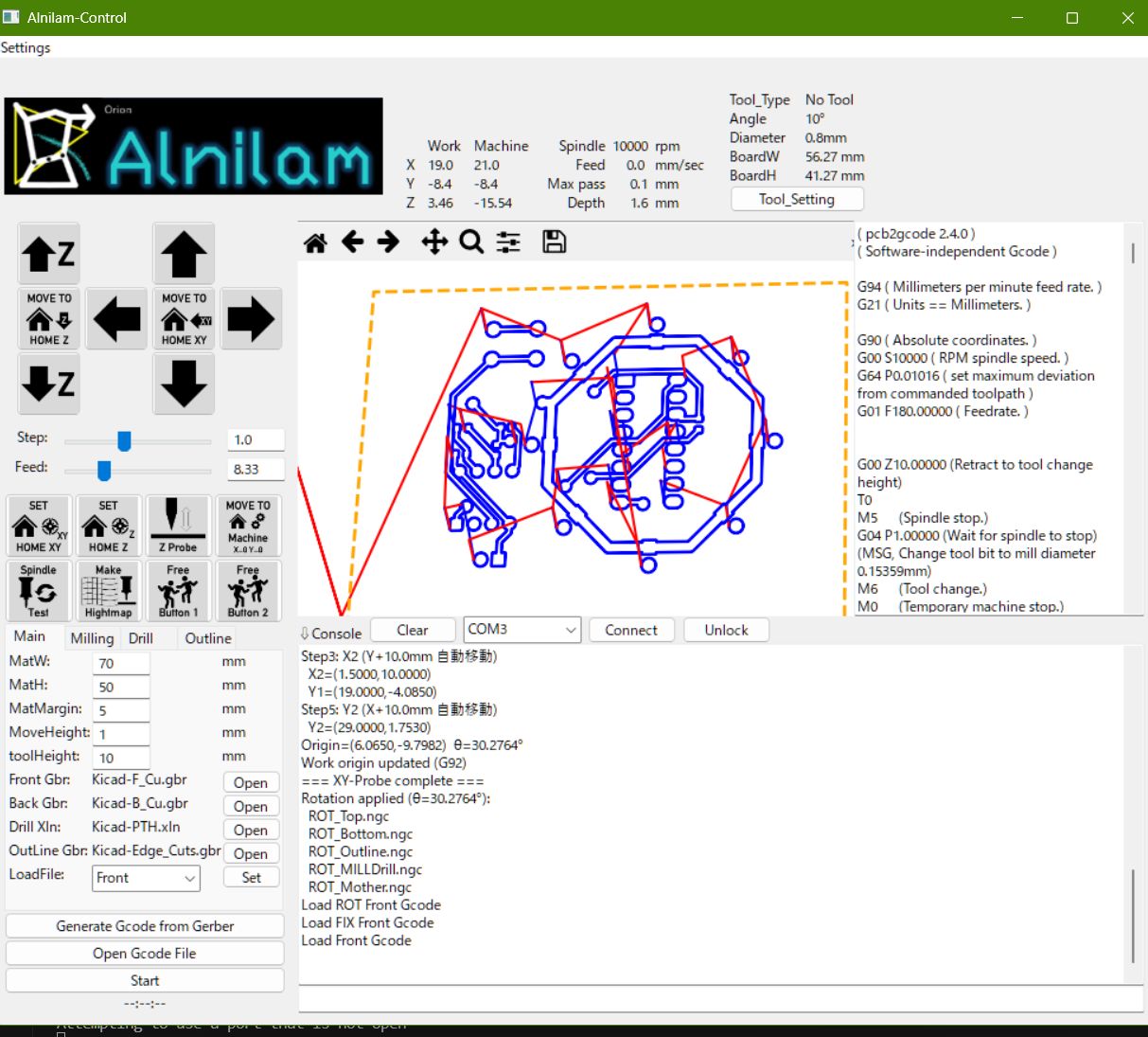 Alnilam Controller, the control app I built in-house
A machine alone is not a tool. I also wrote Alnilam Controller, an in-house Python application that converts the Gerber data exported by KiCad and similar tools into G-code and drives the machine end to end. The experience I am aiming for: load your board CAD data, press a button, and fabrication begins.
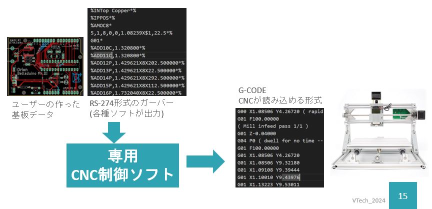 How Gerber data is converted into G-code
Awards and commercialization
Every time I took the machine to an exhibition, it earned recognition and brought in collaborators.
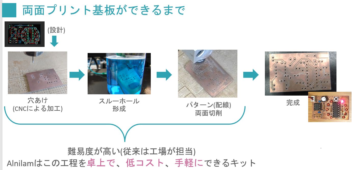 From the presentation slides: how a double-sided printed circuit board is made
In 2021, at Science Castle 2021, a research conference run by Leave a Nest, the project won the 5th THK Award’s Best Development Award and Encouragement Award simultaneously, the equivalent of the grand prize. Through the mentoring that came with the award, specialists from THK taught me how to apply actuators and how to organize development work, and that guidance fed directly into the later designs.
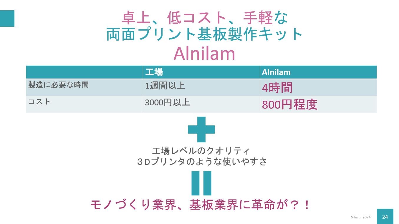 Compared with outsourcing to a factory (a week or more, 3,000 yen or more), Alnilam takes about 4 hours and 800 yen
In 2022 the project took the grand prize in the hardware and embedded category at Geekten 2022. Feedback from student engineers across Japan became the compass for the improvements that followed.
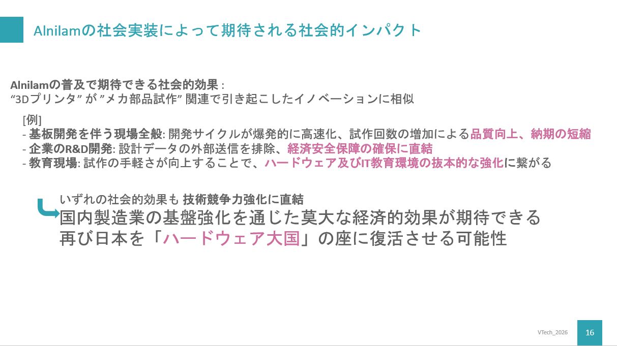 A summary of the effects expected from deploying Alnilam in the real world
After entering university I shifted my weight to the business side. For the 2024 JETRO J-StarX @ Stanford / d.school program I built an English pitch around Alnilam, titled “Trial and Error.”, and examined the room for entry into the US market. Then in 2026, the project was selected for the Kaitaku Course of NEDO NEP 2026. I am now working in parallel on a patent application, developing a kit version, preparing trial kit deployments to high schools, and putting together safety documentation related to Japan’s Poisonous and Deleterious Substances Control Act. I also tested this business hypothesis at the Startup Founders Program (SFP) at the University of Tokyo’s Hongo Tech Garage.